Pcb Height
* pcb locations represent the 0,0 origin of the top of the pcb. //mm/min public const int maxx = boardwidth /.

pcb design I have a doubt on taking pad dimensions in
With the same pcb footprint as all com express standard connectors, there is typically no need to change pcb layouts when making upgrades to your application.

Pcb height. Public const int samplespacing = 5; This tool helps you to calculate weight, area, volume and freigth cost for several types of printed circuit boards (pcbs). About press copyright contact us creators advertise developers terms privacy policy & safety how youtube works test new features press copyright contact us creators.
2.you can accept vague silkscreen if this won't affect your use of pcb. Search our portfolio of free height pcb headers & receptacles for networking infrastructure and select your specifications. //65mm sample width public const int boardheight = 100;
These include 0.031in (0.78mm ), 0.062in (1.57mm) and 0.093in (2.36mm). Being said significant, certain digital applications utilizing higher frequency require controlled impedance. //85mm sample height private const int probingspeed = 60;
//mapping points are 5mm apart. Effects of moisture absorption on dielectric constant (d k ) michael j. Select the checkbox next to use height map so that it is enabled;
Pcb applications, one requirement is the same — pcbs are expected to function according to their design parameters with no errors or. Friday, september 18, 2020 1:54 pm ( permalink ) height: Today, it is more accurate to say there is a range of common or standard pcb thicknesses.
1200*780*1200mm / (50*50)~ (350*250mm) / 250ld 1400. Public const int boardwidth = 70; Just click on the associates banner to save, or enter the associates code at checkout on your next purchase.
It is the combination of capacitance and inductance in an alternating current(ac) characteristic dependent on frequency. •.031" (also.039″ is common) •.062″ (most commonly used size) •.093″ •.125″ For example if we define the max component height for the socket area, as 450 mil then if we place any component whose component height is.
Calculation of printed circuits weight. They have a range of fr4 stock with varying thicknesses that can be laminated to provide a range of thicknesses. From experience, this height could be as much as.5 mm (0.05) which may not seem like a lot, but when routing out pcbs, where the copper layer is on the order of 0.03 mm (.00134) it makes a significant difference, both in the quality of the routed pcb and the ability to do so in the first place.
Pcb impedance every pcb has an important parameter called impedance(z) which is ranging from an average of 25 to 120 measured in ohms. Select the create button under where it says map: within the height map settings, there is a button called auto, which automatically resizes the height map workspace based on your project. When you have a pcb made, you can tell the fabrication company how thick you want the pcb to be.
How to probe the height. Part height should only need to be measured and set once per part. Hi all, if we do not give the component height in the dra file for the component, then what value will be taken for that symbol if it is imported and placed in the board.
For standard boards, multilayer and aluminum pcbs. Today, boards are made to be larger and smaller than this standard, but the standard probably remains the most common thickness for designs. Fill in your pcb's characteristics like.
A part should represent an actual physical sku. Material thickness, copper thickness, material type and layer quantity are all adjustable. These connectors are compatible to pcie gen 4 applications, support 5mm and 8mm stacking heights, and include 220 and 440 position options.
Namespace cnc_command { public class pcbheightmappervm: On the fusion side, open your pcb 3d model, on the timeline on the bottom of the screen right click on the green pcb, then edit. On my router, that works like a charm.
1.it's advised to design the silkscreen height min at 0.8mm, and width min at 0.15mm as our capacity demands. Most pcb materials have methylene chloride resistance values in the range of 0.01% to 0.20%. Want to save 5 to 10% on your next evga purchase?
How the component heights are given. If you have a 47uf cap that is 6mm high and one that is 4mm high, those are different parts. The silkscreen height is 0.5mm,and width 0.1mm,which is beyond pcbway's capaticy.and the silkscreen will look vague on the real pcb.
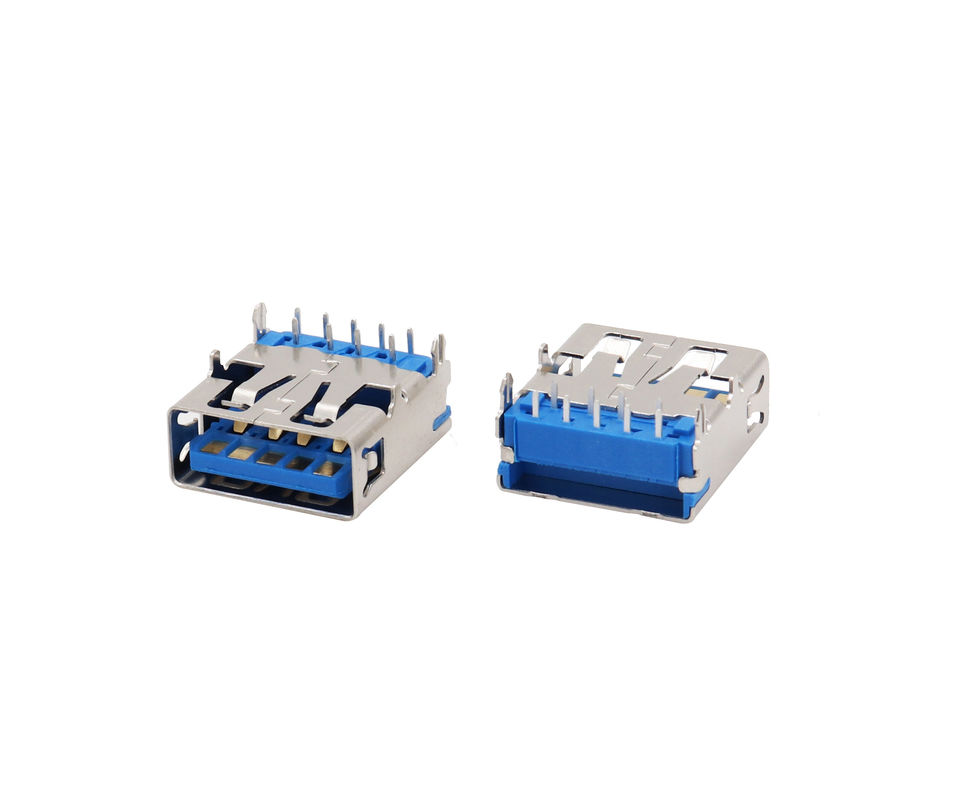
90 Degree DIP USB 3.0 Connector Through Hole Height Over

Low profile spring pins come with above pcb height

pcb How should I lay out timing matched traces

pcb design How can I improve this differential
Hoover Pcb Board, Height Adjust U8361 46851063

12 details that are easily overlooked in the PCB layout

The guidelines of PCB silkscreen design Weller PCB

20 Pin Mini DisplayPort Socket With PCB Standard Height

Shapeoko 2 PCB Height Probing, Milling and Drilling YouTube
Height probing for PCB isolation routing with Eagle/pcbgcode
20 Pin Mini DisplayPort Socket With PCB Standard Height
Horizontal Gecko connectors from Harwin reduce PCB


10pcs Spring Loaded Pogo Pin Connector Through

Distribution of PCBs velocity at each height in Cross Flow

pcb Component Height Altium Designer Electrical
Technical Tips for PCBs Copper Thickness, Controlled
Standard PCB Thickness Importance Of Manufacturing PCBs
PCB footprint dimensions to the world of...

Rule Tips PCB Height Restrictions in Altium Designer